
In this article I would like to illustrate some troubles I’ve encountered using the TMS9918A and how I solved them.
But let’s start from the beginning. In 1979 Texas Instruments commercialised the TMS9918 (called the VDP, or “Video Display Processor”), a video chip that lately was used in the TI99/4 home computer: this chip was able to generate text and graphics at a resolution of 256×192 pixels. Moreover, it was able to generate sprites, aka moving objects that were indipendent from the underlaying background and could be moved around the screen directly by the video chip. The TMS9918 was lately followed by the TMS9918A, developed for the TI99/4A.
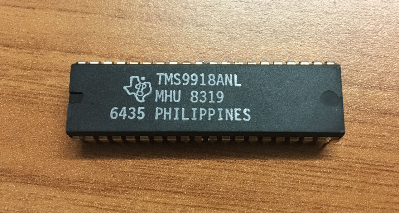
TMS9918A
The TMS9918 had a limit: it didn’t support bitmapped graphics. This meant that it couldn’t handle single pixels on the screen. Instead, it was only able to handle tiled graphics: the image was divided in tiles, each of them was 8×8 pixels in size. But the tiles were only 256 while the image was (256/8=)32 tiles wide and (192/8=)24 tiles high, for a total 32×24=768 tiles. It’s easy to see that an entire tileset couldn’t cover the whole image. This is the motivation that lead Texas Instruments to solve this limit by releasing the TMS9918A: the “A” was for an enhanced version with a new graphics mode where the screen was divided into 3 areas of 256 tiles each, for a total of 768 tiles, so that each video cell of 8×8 pixels had its own tile. By doing so, the VDP had the ability to directly address every single pixel of the image, allowing real bitmapped graphics. The TMS9918A was used in the TI99/4A from Texas Instruments and in a wide variety of systems, i.e. the MSX computers and several Sega game consoles. Unlike the MOS VIC-II from Commodore, that was only used for the Commodore 64 computers, Texas Instruments sold the VDP to a lot of different manufacturers so that it finally became one of the most common video chips of the time. Nowadays it can easily retrieved online for a few euros: for this reason I decided to use it in my little computer.
The VDP can be interfaced with a host processor with just an 8-bits data bus and 3 control lines, no more, no less. Another feature is the usage of a dedicated VRAM, that is out of the address space of the CPU: this means that the VDP doesn’t take off memory from the system RAM. The downside is that the CPU can only access to VRAM through the VDP. The TMS9918A was follwed by the TMS9928A and the TMS9929A: the “28” was basically the same chip but instead of a composite output, it generated a component signal (made by luminance and color difference), while the “29” was the 28 with PAL support (the “18” and “28” were NTSC compliants). So, you could ask me why I chose the TMS9918A if I live in a PAL country… Well, the TMS9929A cannot be connected directly to a TV-in because it doesn’t generate an YPbPr signal but a Y/R-Y/B-Y: the signal is made by luminance (Y) with red (R-Y) and blu e(B-Y) color differences. This means that if I tried to connect the output of the TMS9929A to the YPbPr input of my TV the only thing I could be able to get was a black-n-white picture: I needed an Y/R-Y/B-Y to YPbPr converter. Insted, the TMS9918A can be connected directly to a TV without the need of any interface: the “magic” is done thanks to the fact the almost every modern TV supports both NTSC and PAL standards.
After this introduction to the VDP, I would like to talk about the troubles I encountered while trying to get a decent picture from my computer. The reason is the… VRAM. The VDP was developed at a time when DRAMs were cheaper and more reliable than SRAMs, so engineers chose to embed into the chip the circuitry needed to interface with the formers. DRAMs are not easier to handle than SRAMs: they need also need a negative voltage level (-5V), and have a different way to address their cells. To make a bank of 16KB of VRAM you need 8 16Kx1 chips: these chips are arrays of 16,384 single bits so that to make a single byte of data the VDP has to read 1 bit from each of the 8 chips. Moreover, unlike SRAMs, DRAMs use an address system based on rows and columns: usually, to fetch a data from an SRAM you have to provide the address of the cell on the address bus of the memory. With DRAMs, instead, first you send the row address, then you set the row line, then you send the column address and then you set the column line: only after this sequence has been completed, the chip will return the contents of the addressed cell. Too boring… So I looked around to find a workaround… and I found it. I found a doc by Tom LeMense dated 2010 that seemed to find a modern solution to that: he described a way to interface an SRAM chip to the VDP by using some latches to collect the row and column parts and compose a complete address. The schematic, that you can find in the PDF in my Github repository, lesson 11, didn’t work for me. I don’t know why: simply, I got on the screen the garbage that I published in my previous tests. I looked around the web and it seemed that everyone who used that schematic had success… Eventually, I found another way to wire the VDP to the latches and then to the SRAM, and this one worked perfectly! This schematic has been designed by J.B.Langston for his video board based on the VDP that he developed for the RC2014 computer. As you can see in the image below, he didn’t follow the numeric sequence to wire up the latch outputs to the SRAM inputs (yellow area on the right):
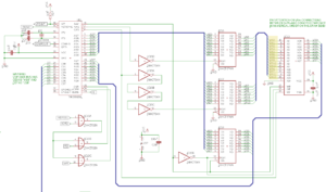
TMS9918A & SRAM
Since the VDP can address only 16KB of VRAM, it uses only 14 lines, divided in 2 groups: 7 bits for the row and 7 for the column, respectively. The circuit stores the row address on the first latch, then the column address on the second latch: at the end, the bits are latched on the output pins to compose the complete address to be sent to the SRAM. Then, the data can be read on the RD7..0 pins directly from the SRAM or written to it through the the third latch (because the VDP outputs the data on the same AD7..0 lines).
I don’t know why and I don’t know how he found that he had to change the sequence of the address wirings but I surely know that it works. My computer now shows its shining name in the top left corner of the screen:
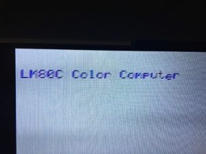
LM80C-welcome message
There are some things to consider:
- follow the wirings between the latches and the SRAM;
- don’t forget that the VDP, like the processors from TI of the time, considers the bit #7 as the LSB and the bit #0 as the MSB, so you have to invert the pins of the data bus: connect from D0..D7 to D7..D0;
- since the data on RD7..RD0 must be stable before the column line is set up, the original author used a daisy chain of 3 NOT sections to achieve some delay;
- it is critical that there is a path between the RDx pins of the VDP, the IOx pins of the SRAM and the ADx pins: so double check that each pin is connected to the corresponding number in the chain (i.e. AD0 is connected to VD0 through the connection that passes in the third latch between 1D and 1Q);
- don’t mix LSxx with HCTxx chips: as the timings are fundamental, use ICs from the same family;
- another CRITICAL point is the frequency of the clock signal: the crystal must be a 10.738635MHz one, with a very low tolerance (+/-0.005%). It is not very common but you can find if you look around a little bit. The frequency is mandatory: it’s used to generate the internal clock that the VDP need to operate, including the 3.579545MHz clock used to generate the color burst, the signal that carries the color informations in the video signal. Another thing to keep care of are its capacitors: a value of 33pF should be good enough for any circuit (the datasheet suggests a value between 15 and 39pF, depending on the stray capacitance of the circuit).
As usual, the schematic and the code are on my Github repository.

I found some MK4516 Drams in my junkbox. These are 5v only versions of the 16Kx1 16 pin 3 voltage kind. I should be able to use these without the SRAM conversion circuit. Technically though there might be fewer solder connections with the SRAM circuit. I have a sample WD9918A chip I got years ago, Western Digital second sourced the VDC (as did a few others).
I’m happy that you found my writeup of using SRAM with the VDP, but I’m sorry to hear you had problems getting it to work. I recall when I was doing the original adaptation to SRAM that the TMS9918 and TMS9928 timing is very ‘rough’ – two things come to my mind after I read how you solved the issue by re-ordering address lines: 1) the internal structure of the SRAM is rows and columns, and the access time for each isn’t really the same; there could be a ‘race’ between them. 2) perhaps the speed of the SRAM makes a difference – I used old 80486 motherboard cache RAM chips, which are quite fast – 15~20ns of access time. The VDP cycle is quite long, so even a much slower SRAM should work, but the setup/hold times required by the SRAM often scale with the access time, so it could be related to this. I’d be curious to hear your thoughts on this, and if you think that SRAM type/speed might be the factor…
-tom
(Tom LeMense)
Hello Tom, I’m happy to see that you found my project and that I used a work of yours, too. I really don’t know if the issues I experienced can be related to RAM timings (I don’t have an oscilloscope to check it). I used 120ns SRAMs, I thanked they could be fast enough to output data to the VDP, but reading what you wrote, it seems that I’m an order of magnitude over the required timings…
All of the credit for my design must go to Tom since I used his design verbatim. All I did was add address decoding and lay it out on a PCB. I am not sure why my circuit worked for you his didn’t because they are in fact the same circuit. If you read Tom’s PDF carefully he states that the order of the address lines do not matter. The only reason I ordered them the way I did was because allowed the most straightforward layout of the tracks on the PCB without any crossovers.
That’s very strange… I will do some other tests to check why my circuit only works following your schematics and doesn’t replicating Tom’s one… Thank you for the feed