Once I chose the CPU, I started studying it. Altough I used 8-bits computers, at the time I was too young so I never tried to build or design one of those system. Fortunately, the choose of a very common CPU has been rewarded and internet is full of resources for the Z80, so it was not difficult to find what I was looking for. Moreover, Zilog still continue to produce and sell the Z80 processor so finding up-to-date informations was an easy task.
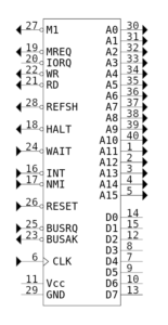
In the picture below you can see the pinout of the Z80 processor:
Here is a brief description of the pins that I will use for my purposes:
- address pins A0..A15: as you can easily figure out, these are the pins that are used to “address” the memory. It means that they are used to specify the physical address of the memory location where the CPU wants to read from or write to a data.
- data pins D0..D7: these pins are used to transport the data from/to the CPU.
- M1: this is a particular pin. To understand its function, we have to first understand how the Z80 works. It does not operate by single clock signals but by machine (M) cycles, 3 M-cycles for each instruction. The first machine cycle is called “M1” and it is used to fetch the instrucion to be executed from the memory. M1 pin, in conjunction with MREQ, indicates that the CPU is fetching the instruction. It is also used with IORQ to indicate that an interrupt have been acknowlegded.
- MREQ: this pin indicates that the address bus is holding a valid address for a reading/writing cycle from/to the memory.
- IORQ: this pin indicates that the first 8 pins of the address bus (A0..A7) are holding a valid peripheral address.
- WR: it indicates that the CPU wants to write (WR stands for Write) to a memory address or a I/O peripheral.
- RD: it works in a similar manner as WR but for reading operations.
- REFSH: almost useless. It was used to refresh Dynamic RAM (DRAM) but today Static RAMs (SRAM) are cheaper and don’t need refreshing cycles anymore.
- HALT: the Z80 CPU can be halted in its operating functions. While it’s halted, it still continues to execute NOPs operations to refresh the memory while it waits for an external interrupt signal to restart its activities.
- WAIT: this pin was useful when memory were slower than the CPU, so this pin could be used to let the CPU wait for the memory to complete the reading/writing operation.
- INT and NMI: these are the interrupt pins. The pins indicate that the CPU should execute specific interrupt routines. The difference between the 2 is simple: while INT is maskeble, meaning that the user can set a flag to let the CPU ignores the INT signal, the NMI interrupt isn’t (NMI means Non Maskable Interrupt) and it will be always honored.
- RESET: this pin is used to reset the CPU.
- BUSREQ and BUSACK are used to share the data and address buses with external peripherals. The first one indicates to the CPU that an external peripheral wants to keep control of the buses while the second one indicates that the CPU has just left the control of such buses.
- CLK: this is the clock input. The clock is a special signal: it alternatively goes from high to low. The clock signal is used by the CPU as a timing to synchronize all of its internal operations. It’s like an orchestra leader that give the time to all the components of the band. The maximum frequency of the clock depends on the CPU type: the original Z80 can runs at frequencies up to 2.5 MHz, the Z80A up to 4 MHz, the Z80B up to 6 MHz, and the Z80H up to 8 MHz. More recent versions are able to run to 10 and even 20 MHz. My Z80 is a “B” model.
For my purposes I will ignore several pins. I will just use the address and data pins (obviously…), the IORQ and MREQ pins with the RD/WR pair, the clock pin and, maybe, the INT and NMI pins.
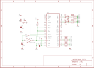
But before to proceed I had to test my CPU. Since my Z80 was an used processor I had to verify that it was a working unit. To do that I found on internet a very simple test. Let me explain how it works. When the CPU is powered up it load into its program counter (PC register) the address $0000, then it jumps to that address, read the instruction stored at such location and executes it. The simplest instruction is NOP, that stands for “No operation”. This is a “dummy” instructions: the CPU does nothing during the machine cycle apart to increment the PC to load the next instruction. The op-code, the numeric value that represent this instruction, is $00: if we set the data bus so that the CPU reads a $00, we are telling the CPU that the instruction to be executed is just NOP. To do that we can simply connect the data pins to ground so that the CPU will read 8 low values. To see that the CPU is working we can connect several LEDs on the first address pins: since the NOP is like a placeholder, the CPU increments the PC to recover the next instruction from the system memory. This should lead to the memory address that is increased endlessly. If we use a very slow clock we can look at this in the form of a binary counter with the LEDs that light on when the address pins are set to an high level (a “1”) and light off when set to a low level (a “0”). Thanks to the ability of the Z80 to run at very, very low frequency clocks, we can build a simple RC oscillating circuit and a 7414 Schmitt-trigger NOT gate to generate the square wave that the CPU is expecting for on the CLK pin. The schematic is below:
The CPU address pins are not very robust so they can just source a limited current: for that reason I connected the LEDs with a high value resistor to be sure that the current will be limited to a very low amount. I used 680 ohm resistors that, for red LEDs, correspond to a current of about 2.5 mA each pin. Same for the data buses: I didn’t connect them directly to ground but I used pull-down resistors of 1K ohm. I uses a 74HCT14 Schmitt-Trigger hex inverter (a NOT gate) to generate the square wave clock: it triggers only when the voltage on the input pin goes under or over certain values, so that it doesn’t trigger for mimimal fluctuations in the signal. With the above circuit the frequency is 12 Hz, but you can use different values for R1 and C1 to get different oscillating times, that mean different clock speeds. I added a reset button because the CPU need a stable clock before it can work correctly: when we power up the circuit small oscillations in the voltage could lead to unpredictable behaviours. So it is reccomended that once we power up the circuit we apply a reset signal for at several clock cycles. This is not necessary if you use a dedicated reset chip or a different circuit based on a NE555 timer used in a monostable circuit, as we will see later.
Here you can see how the test looks like:


